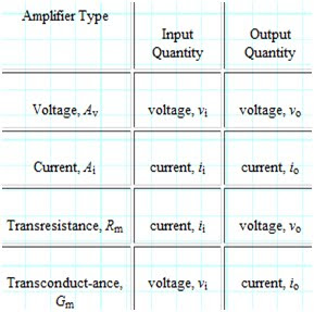
In the table under amplifier type is the expression for amplification or gain (or transfer function), which is the output quantity divided by the input quantity. In general, A = xo/xi, where x is either a voltage or current.
An ideal input port is not affected by input source resistance nor is an ideal output port affected by output load resistance. The general amplifier is shown below:
The combination source/resistance symbol is a generalized source: either a Thevenin or Norton equivalent circuit. The amplifier has an input resistance Rin and output resistance, Rout. The input source, xi (where xi is vi or ii), has resistance Ri. It forms a divider (voltage or current) with Rin so that xi ¹ xin. Similarly, output resistance Rout forms a divider with output port load resistance RL so that the output xout = K× xin ¹ xo. The amplification of xin by K results in xout that is K times larger. K is the gain, and it scales xin. (Gain less than 1 is called attenuation.) If source or load resistance is unknown or varies with K, then error in the overall amount of gain results. An accurate (or at least unchanging) gain is required for calibrated sensor circuits, so that the transducer output is multiplied by a known (and constant) amount.
An example of a voltage amplifier is shown below:
The first factor is the input voltage divider attenuation, the second is the amplifier voltage gain and the third is the output voltage divider attenuation. For the ideal voltage amplifier, Av = K. This is achieved when Rin approaches infinity (open-circuit input) and Ro = 0. The ideal port resistances are given in the following table:
In practice, good amplifier design approaches the ideal so that input and output loading does not affect the overall amplifier gain accuracy.


No hay comentarios:
Publicar un comentario